


Description
About the Circuit:
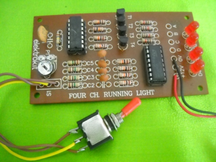
The circuit is build around shift register IC3 as shown in the circuit diagram. It has eight outputs. The output goes on shifting at every clock pulse at pin1 and pin9. Each register has independent CLOCK and RESET input as well as a single serial DATA input. The logic level present at the DATA input is transferred into the first register stage and shifted by one stage at each positive going clock transition. Resetting of all stages is accomplished by a high level on the reset line at pin14 and pin6.
The clock circuit is designed using astable multivibrator IC1. The frequency of clock pulse is determined by timing components R1-R2/P1-C1. The frequency of oscillation can be changed by adjusting preset P1. Data input at pin7 of IC3 is provided by IC2, which is also an astable multivibrator. Preset P2 is adjusted for correct logic data input.
Each eight output drives transistor T1 to T8 respectively. And each transistor drives 11 LEDs connected at the collector terminal. At first clock pulse output at pin5 of IC3 becomes high and T1 turns on, which drives 11LEDs. At second clock pulse pin4 of IC3 goes high and T2 turns on. In this way output goes on shifting at every clock pulse.


Reviews
There are no reviews yet.